In this lab we are going to experiment with gates and circuit design. We’ll use our understanding of gate behaviour to design a half adder and a full adder circuit, each of which will be implemented on the breadboard and interfaces with the Raspberry Pi.
The 74xx Series
The 74xx series of chips generally contain logic gates and other components. For example, the 7402 chip contains 4 NOR gates on a single 14-pin chip. There are many variations, including some that have memory (flip-flops, latches). The table below summarizes some of these chips.
| Base Model | Description |
|---|---|
| 7400 | Quad 2-input NAND gates |
| 7402 | Quad 2-input NOR gates |
| 7404 | Six 1-input inverters (NOT gates) |
| 7408 | Quad 2-input AND gates |
| 7432 | Quad 2-input OR gates |
| 7486 | Quad 2-input XOR gates |
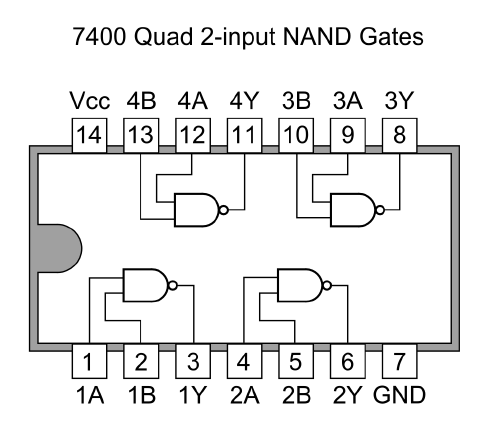
Nearly all of the above chips have an identical pinout (the exceptions are the 7402 and the 7404). The diagram below illustrates the pinout of the 7400 chip.

To use one of these chips, connect pin #7 to ground, and pin #14 to +3.3V. You may then connect two inputs (either GPIO output ports or directly from power source) to pin #1 and pin #2, and connect the output (pin #3) to either an LED (with an appropriate resistor) or a GPIO input port.
You can also combine gates together by connecting output pins to input pins.
Half Adders
A half adder is a circuit that adds two binary digits, producing a sum and a carry bit. The carry bit is one when the two bits add up to more than can be stored in a single digit. This happens when both input bits are one (high), which produces a zero (low) sum bit and a one (high) carry bit.
Circuit Design
One can easily construct a half adder for two input bits (X and Y) by drawing the truth table for both sum (S) and carry (C), as shown below.
| A | B | S | C |
|---|---|---|---|
| 0 | 0 | 0 | 0 |
| 0 | 1 | 1 | 0 |
| 1 | 0 | 1 | 0 |
| 1 | 1 | 0 | 1 |
Recognizing that the S column is identical to the truth table for XOR, and that the C column is identical to the truth table for AND, we can design a very simple circuit for a half adder.

Hardware Setup
Take out the Raspberry Pi and lay it on a flat surface. Identify the 74xx chips required by examining the model numbers written on the top of the chip. You will need a 7408 (quad AND gate) and 7486 (quad XOR gate) for this part. Each of the two chips must be mounted across the gap in the middle of the breadboard, so that each side of pins has its own breadboard column for connecting wires.
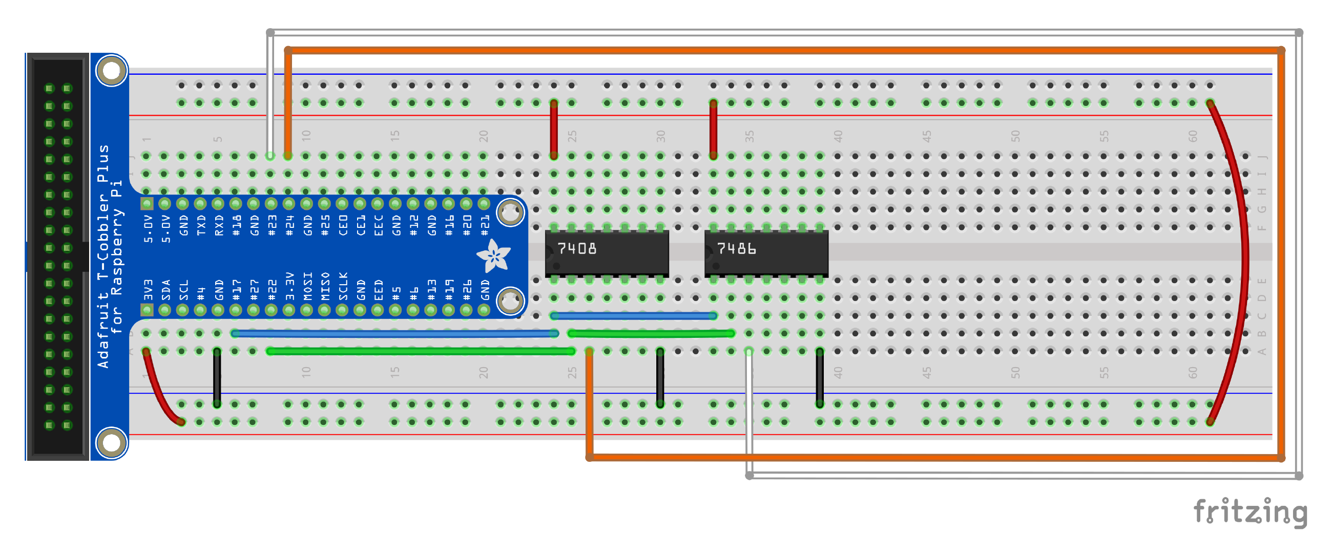
Connect a red wire to a power supply of +3.3V on the GPIO header, and plug it into the red line at the top of the breadboard. This will supply power to both chips. Connect a black wire to one of the ground GPIO pins, and plug it into the blue line at the bottom of the breadboard. For each of the two gate chips, plug another red wire from the red line to pin #14 (top left) on the chip, and another black wire from the blue line to pin #7 (bottom right) on the chip. This will power the chips.
Now, connect the inputs for both the first XOR gate and the first AND gate to the GPIO17 and GPIO22. Connect the output from the XOR gate to GPIO23, and the output from the AND gate to GPIO24. The completed circuit wiring is shown below.

Exercise
Write some code in Python to test your half adder circuit will all possible inputs. A template has been provided below:
import RPi.GPIO as GPIO

GPIO.setmode(GPIO.BCM)

# GPIO 22, 17, 23, and 24, respectively
(A, B, S, C) = (22, 17, 23, 24)

GPIO.setup(A, GPIO.OUT) # GPIO #22
GPIO.setup(B, GPIO.OUT) # GPIO #17
GPIO.setup(S, GPIO.IN)  # GPIO #23
GPIO.setup(C, GPIO.IN)  # GPIO #24

print("A B S C")
print("-------")

for a in [False, True]:
   for b in [False, True]:
      # test a,b inputs

GPIO.cleanup()
